SERVICES
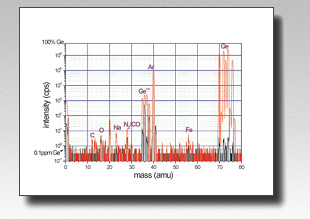
SNMS spectrum of a "pure" Ge-sample taken with an Ar+ ion bombarding voltage of 1.4 keV (red) in comparison with the signals for ion bombardment at about 30 eV (black). Note the low mass independent background of 4·10-1 cps and the signals in the "residual gas" range. The C-signal refers to a carbon impurity of about 11 ppm in the Ge-sample.
The SNMS System INA-X is especially developed for extreme depth resolution and therefore ideally suited for applications in thin films investigations.
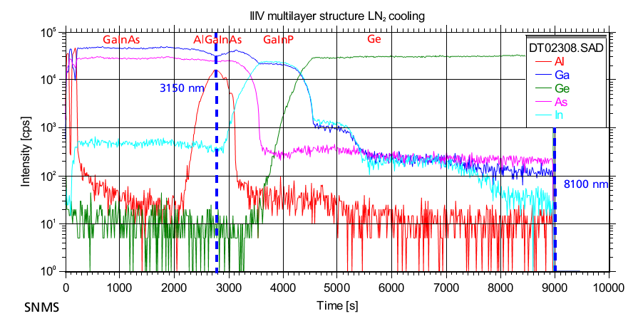
Shown are recent data ion GaAS/AlGaAs/GaAs/GaAs/AlGaInAs/AlGaInAs/InGaAs.
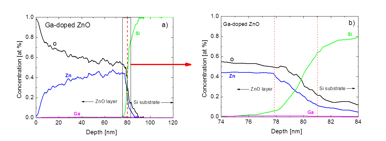
SNMS depth profile for ZnO on Si showing the strong variation of the concentrations at the interface and the extremely high depth resolution.
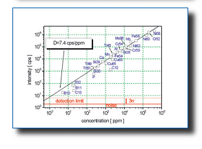
SNMS intenstity as a function of the specified concentration in a standard sample (NBS 1245a). Most of the elements are detected with similar sensitivity demostrating the already quantitative behavior of the raw data. An SNMS signal of 7.4 cps per ppm demonstrates a detection limit below 1 ppm.

SNMS depth profile of antireflective on optical glass. The intrinsically present electrons in the plasma can be used for charge compensation in the sputter processes. This allows easy reliable analysis also of insulating samples like ceramics or glass. Below an example of analysis of antireflective coatings on optical glass is shown.