SEM-FIB MICROSCOPY
In this unit we offer imaging, analysis and control of matter at the nanoscale — keys to future research and development — from the use of the Helios Nanolab 650 microscope. This SEM/FIB combines the most advanced scanning electron microscope (SEM) and focused ion beam (FIB) technologies with innovative gas chemistries, detectors and manipulators. Featuring unsurpassed SEM resolution, image quality and stunning Tomahawk FIB performance, imaging, milling or preparing samples is fast and easy for semiconductor and data storage labs, research facilities and industrial applications, some of which are described below.
 |
 |
 |
 |
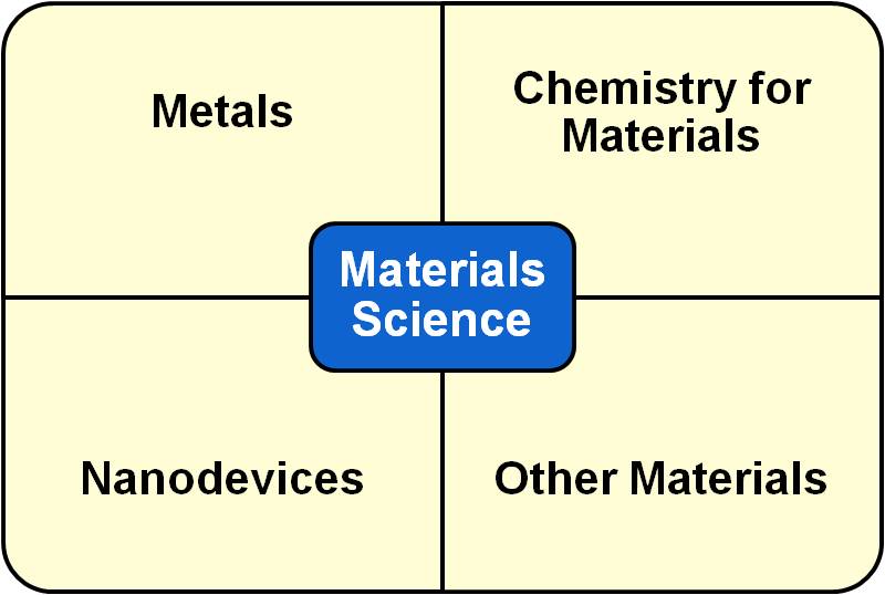
| Micro/nanomachining In-situ electrical measurement TEM sample prep Circuit editing Nanophotonic structure fabrication |
Cross-sectional imaging Nanowire research |
